What we do
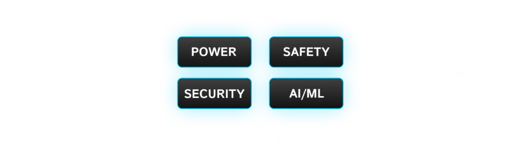
Specifications, Microarchitecture, RTL Design: SoC level IP integration including processors (Arm, RISC-V), AI subsystems (ISP, GPU, NPU, etc.) and IPs (DDR, PCIe, USB, etc.) and RISC-V extensions.
Design Verification (DV): UVM based verification of SoC, sub-system IP level (specifically Arm/RISC-V) based and other high speed and low speed IPs. Emulation friendly UVM verification infrastructure. Advanced flow development, coverage closure (line, branch, interface toggle, functional, etc.) to meet very aggressive project schedules.
Physical Design (RTL2GDSII): Synthesis (SDC, CDC, STA, PPA analysis, DFT), floorplanning (including feasibility), placement, clock tree synthesis, routing, electromigration and IR delays, DRC/LVS and signoff (timing, power). Targeted to meet PPA (power performance area), enable refinement/convergence and signoff closure at advanced process technology nodes (16nm, 12nm, 10nm, 5nm) working with foundries (TSMC, Samsung).
Our optimized flows at advanced FinFET process nodes (TSMC, Samsung), using industry leading tool flows to meet PPA and cost, reliability and EMIR, faster design closure and time to market (TTM) goals.
Arcana Semiconductors Successes
Multiple SoC tapeouts and IP hardening projects at 16FFC, 12FFC, 10nm and at 5nm. At the SoC, sub-system, block and IP level.
Applications: Edge AI, IoT, Wearables, AR/VR, AI, Automotive, 4G/5G, Embedded, Mobile, Security, Video compression, Memory, etc.
IP: RISC-V and Arm based processor IP high end to microcontrollers (microarchitecture, RTL, Design Verification, Physical Design), AI subsystems, DDRx, MIPI and other IPs.
VIP: UVM based on reusable VIPs
Flow development: UVM based DV. Physical design 16FFC, 12FFC, 10nm, 5nm (TSMC and Samsung).